Recently, I have been working on the muNico 32 which is a custom form-factor of development boards while development on the PicUNO has been halted temporarily due to many regulatory factors while the board continues to undergo testing.
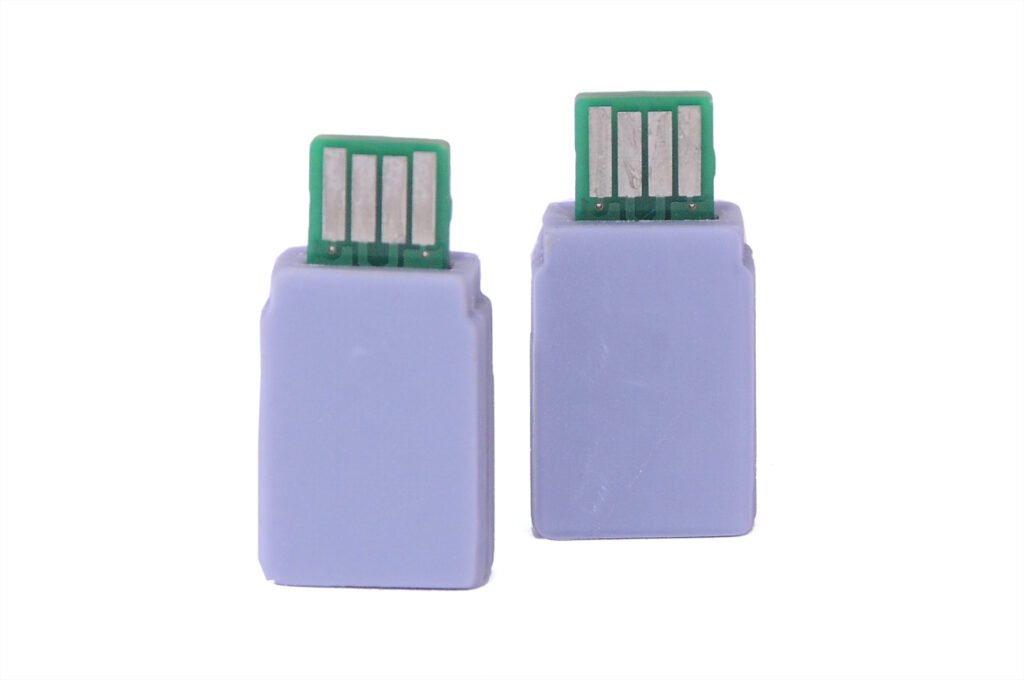
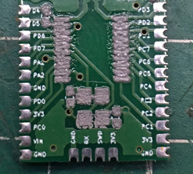
The muNico is a very small USB pen-drive sized board and hence using a soldering iron to manually solder each pin of the CH32 is a herculean task. To combat this, I decided to use solder paste. At first, I bought a syringe of Relife paste from a local supplier. And at this point I did not have a stencil at hand. So, I just added a thin line of paste on the PCB which ended up leading to several issues when reflowed with my custom hotplate. One of the major issues was solder bridging and the other was bad flux stains.
Combating the flux stains is easy and I did this by using some Isopropanol and Acetone or by just changing the paste. But the issue with bridging can only be fixed if adequate amount of paste is added. And to do so, I placed an order of a stencil from my PCB Supplier PCB Power. And this arrived in a few days’ time in good shape.
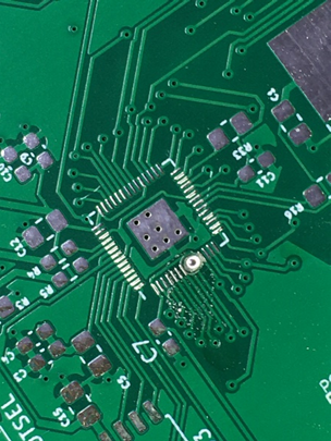
OF PASTE ADDED WITH STENCIL (Image Source: Microcontroller developed by Atul Ravi)
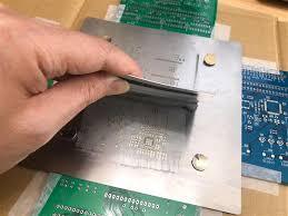
Now came the task of placing the stencil on the muNico board. Mind you, the board is very small. So, placing many muNico boards around the one to be stencilled is not an appropriate option as it will waste PCBs and time. So, I thought of using other PCBs which lead to the issue where the other boards were 1.6mm thick. But the muNico to adapt for the USB A port, is 2mm thick.
So using other PCBs to hold my PCB like the image below was completely out of question.
This forced me to consider what could be done to fix this. In the end, I decided to 3D print a jig. But as my board is abnormally shaped, modelling will be tough. So, I exported the PCB file as a wrl file which I could import into blender.
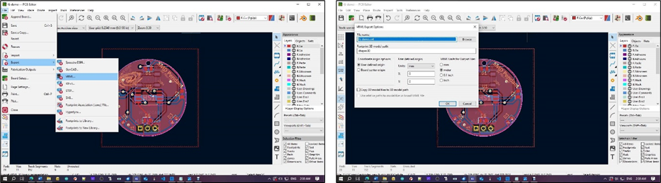
(Use the image above as reference to import the .wrl file from KiCAD)
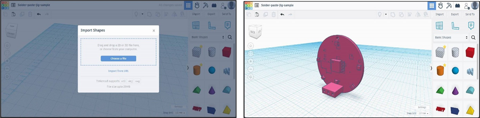
After importing into blender, I decided to export it as an STL that I could open with CAD software of choice (Tinker CAD). Now proficient users of Blender need not export to a separate file to do this task, but I decided to do so as my knowledge of blender is equal to that of a rock.
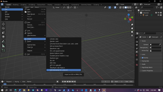
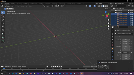
When the file is imported, its scale will be extremely small. To combat this issue I created a new collection
Selected all individual parts while pressing shift and dragged them into new collection as shown.
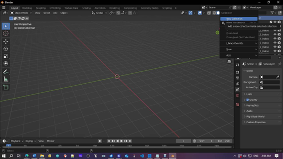
Now pressed ‘s’ key and scaled up the imported file to my requirement.
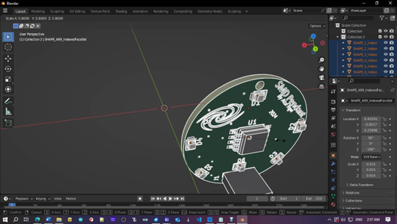
This is the reference of how the scaled model looked.
After selecting all parts in the collection, exported the part as a STL file by navigating in blender as shown below.
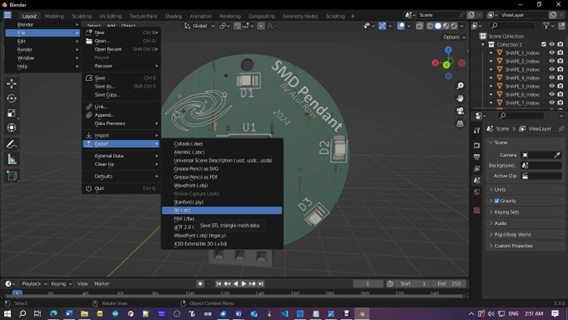
This image is used as reference to export the file as a STL.
After importing into Tinker CAD, I let the model remain and created a cube 2mm thick and slightly bigger than my stencil. Then I converted the model into a hollow so that I can merge it to remove the area of the PCB. (If you are comfortable with using blender, you may use the same for the steps below too. However, I assume that you are using a PC that will run TinkerCad better than blender and hence use it in the steps that follow.)
The above step is slightly complicated as the size of the board exported from Blender, will not be the appropriate size. So, you will have to ensure that it will be of the perfect size so that the jig will work perfectly.
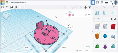
Then, I added a Cuboid. that was slightly bigger than my actual PCB, converted the model to a hollow and removed the PCB area from the Cuboid.
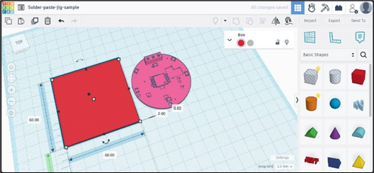
Cuboid slightly larger than the PCB added.
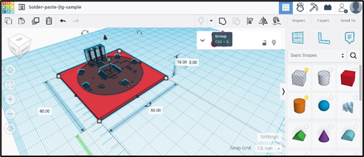
The PCB model is converted to a hollow and both models are merged.
After I removed that area of the board on the 3D model, I exported it and sent it over to my ender 3.
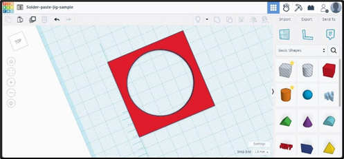
The jig is now ready. And is downloaded.
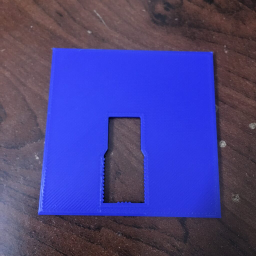
And after roughly 2 iterations, I was left with the perfect jig. (The jig might look different from what is illustrated above as the model used is of a different project for reference purposes only.)
In the end, I pasted the jig to a thin wood piece included with the stencil and used tape to attach the stencil after using the PCB on the jig to ensure that it was aligned correctly.
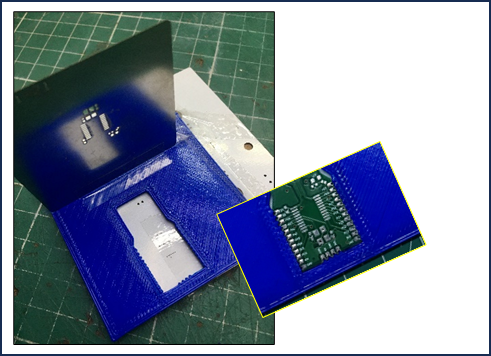
What I now had was the perfect jig for my oddly shaped PCB on to which I could now apply the solder paste with ease.
To actually apply the paste, I used a very old plastic card. However, you may print out a squeegee which can also be used to effectively spread the paste over the PCB. I recommend the Prusa, print remover tool which is a single print which will have a good result. Download the model from here.
The common hobbyist might ask, why not cut the wood included with the stencil? Yes, I could have done that. But in my case, it was slightly thinner than the board and was also extremely hard to cut into. It is not like I did not attempt to do so. But it was mostly in vain. And what about cardboard? Yes, that is an excellent option if you find carboard of the correct thickness. But for a large assembly run, a proper Plastic jig will be much more useful than carboard that might flex under weight.
To conclude, this was how I utilised my 3D Printer to create a solder paste jig at ease. And you can do so too. If you found this interesting and/or useful, please feel free to share to anyone who might also find this trick interesting.
(Note: The circuit board illustrated in the Blender and TinkerCAD examples are not that of muNico but is from a different project which can be viewed here. https://github.com/atulravi/Ki-demo )
Leave a Reply